標準プロセス?
- NanoWiring: 表面に金属ナノワイヤを成長させます。
- KlettWelding: 両面ナノワイヤリング構造。
- KlettSintering: 一方の面だけがその構造を持っている。
- KlettGlueing: 敏感な電子部品のため。
- KlettWelding Tape: テープおよび巻き枠の包装で利用できる。適用と保管が簡単。
説明
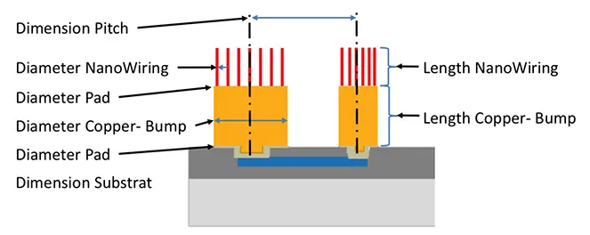
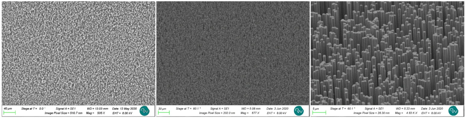
NanoWiringの直径と長さを教えてください?
NanoWiring の直径は 30nm から 4µm の間で調整できます。
ナノワイヤーの長さは、1μmから50μmです。
NanoWiresの直径や長さはどのように制御しているのですか?
ナノワイヤの直径と長さは、スポンジ材料の多孔性層によって定義されます。
ナノワイヤの寸法は、SEM またはデジタル顕微鏡で測定できます。
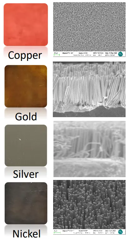
ナノワイヤーの素材は何ですか?
- 多様な金属のナノワイヤーを作ることができる。
- 可以生产出多种金属的纳米线(铜、金、银、镍等)。
- コア材料は、導電性 (金属) または絶縁体 (カプトン、PTFE、ゴム、セラミックなど) にすることができます。
ナノワイヤーの製造に使用されるスポンジ素材は何ですか? 有機物ですか、それとも無機物ですか?
有機素材
多孔質基板材料をどのように作成しますか?
スポンジの多孔層は、特殊なプロセスによって作成されます。
多孔質基材はどのように剥がすのですか?
労力を軽減するために、多孔層の領域を除いて、スポンジ材料の一部を機械的に除去します。 次いで、シクロペンタノンを用いて湿式化学的に多孔性層領域を除去する。 これは、自動化された多段階洗浄プロセスで行われるため、残留物を残さずに除去されます
- 最も高い生産の速度
- SEM像の一例
- 両面ナノワイヤリング構造
- プロセスパラメータ: 室温, 圧力(15 MPa から), 時間(60 ms から)
- せん断強さ(15までのMPa)

- フリップ・チップ (Flip Chip)
- 温度に敏感な機器
- FPC/PCB, PCB/PCB
- ダイアタッチ(ダイボンディング)
- 大電流母線
- 高い剪断強度
- SEM像の一例
- 両面ナノワイヤリング構造
- プロセスパラメータ - 温度(170°Cから) - 圧力(10 MPa から) - 時間(10sから)
- 圧力(60 MPa から)
- フリップ・チップ (Flip Chip)
- 温度に敏感な機器
- FPC/PCB, PCB/PCB
- ダイアタッチ(ダイボンディング)
- 大電流母線
- 低圧プロセス, 低温プロセス
- SEM像の一例
- 両面ナノワイヤリング構造
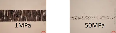
- プロセスパラメータ - 低温プロセス - 圧力(1 MPa から) - 時間(60sから)
- せん断強さ(10...50 MPa)
- フリップ・チップ (Flip Chip)
- 温度に敏感な機器
- FPC/PCB, PCB/PCB
- ダイアタッチ(ダイボンディング)
- 大電流母線
NanoWired は現在、次の材料で作られた KlettWelding-Tape を製造できます:
- コア主要材質: ほとんどの金属 (標準材質は銅), polyimide, etc
- コア厚 Cu: 5µm, 20µm, 100µm,... 2mm (標準 = 20µm)
- コア厚 polyimide: 12µm, 25µm, 50µm
- NanoWiring 直径: 30nm,... 4µm (標準= 1µm)
- NanoWiring 盛り土の要因: 10%,... 40% (標準=18%)
- NanoWiring 材料: 銅、銀、金、ニッケル(標準=銅)
- ハイブリッド設計も可能(ニッケル/銅、銅/銀など
- 銅ナノワイヤーにはさまざまな品質クラスが用意されています (標準、プレミアム、特別)
- 電気的絶縁Klettwelding Tapeも利用可能
- We use polyimide as insulation material for insulation Velcro welding tapes.
- The usual thicknesses are possible:
- Asia: 12 µm
- Europe: 25 µm (dielectric strength 7.8 kV)
- Additional: 50 µm / 75 µm
- Particularly when power electronics assemblies and components are used, they are SHIELDED with a SILVER SURFACE.
- In order to connect such modules and assemblies to a copper-clad PCB, NanoWired GmbH has developed a hybrid Velcro Welding Tape with an integrated diffusion barrier.
- One side of the surface is SILVER - NanoWiring and the other side consists of copper NanoWiring. This makes it possible to directly connect two substrates with differently metallised surfaces using VelcroSintering. metallised surfaces using VelcroSintering+.
- Penetration and infiltration of the copper by silver atoms is reliably prevented by the nickel diffusion barrier.
- Yes, with the KlettWelding tape the destroyed connection between two components can be restored. This does not require a new surface treatment with NanoWiring.
- KlettSinter+
A new connection can be made by Velcro sintering with Velcro Welding Tape (from 170° C). Whether 6″" or 8″ is irrelevant for the dispenser application, but certainly a know-how-relevant process. - KlettGlueing+
Alternatively, the mechanical strength can also be achieved by gluing, the KlettWelding-Tape provides the electrical contact of the components.
- The used base metallization and the materials of the NanoWires have differences in their length variation.
- The quality of the electrolyte used can also influence the homogeneity.
- The distribution and diameter of the NanoWiring structure have a negligible scattering.
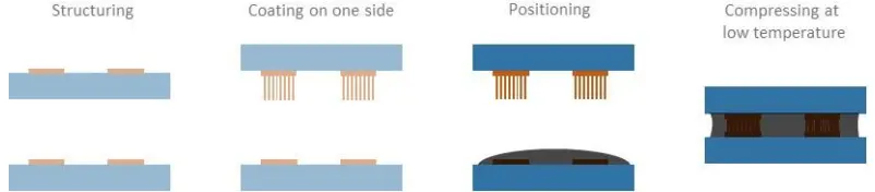
Higher bondline thickness
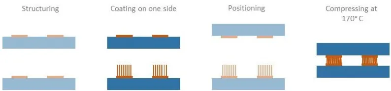
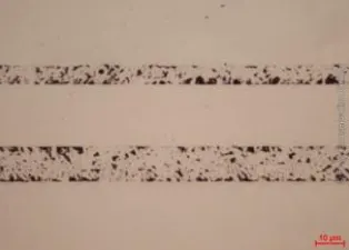
- SEM cross-section structure
- Preparation
- Both surfaces have a NanoWiring structure
- Use of KlettWelding Tape - Conditions of the connection
- Room temperature
- From 15 MPa
- From 60 ms - Result
- Extended bondline thickness through the use of Velcro Welding Tape
Most cost-effective method, high-strength connection
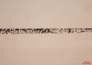
SEM cross-section structure
- Preparation
- Only one surface has a NanoWiring structure - Conditions of the connection
- From 170°C
- From 10 MPa
- From 10 s - Result
- Shear force level approx. 50 MPa
- Automotive Busbar Power transport by car/plane/truck
- Housing technology
- Power Electronics / Die Attach
- Contact link
- Ceramics on metal (e.g. sensors)
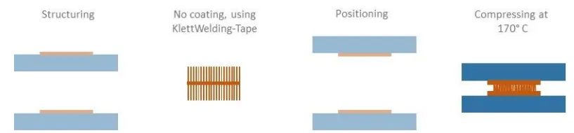
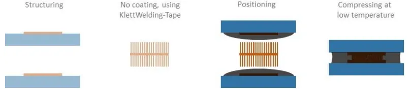
Minimum preparation effort, high-strength connection, repairable
SEM cross-section structure
- Preparation
- No surface has NanoWiring structure
- Use of KlettWelding Tape - Conditions of the connection
- From 170°C
- From 10 MPa
- From 10 s - Result
- Shear force level approx. 50 MPa
- Automotive Busbar Power transport by car/plane/truck
- Highest flexibility
- Placement
- 3-D electronics
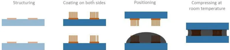
Higher bondline thickness
SEM cross-section structure
- Preparation
- A surface has a NanoWiring structure
- Use of KlettWelding Tape - Conditions of the connection
- From 170°C
- From 10 MPa
- From 10 s - Result
- Increased bondline thickness through use of KlettWelding Tape
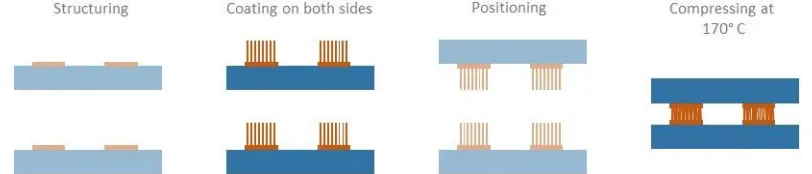
Low binding force, low temperature
SEM cross-section structure
- Preparation
- A surface has a NanoWiring structure
- Use of low viscosity adhesive - Conditions of the connection
- Low temperature
- From 1 MPa
- From 60 ms → depending on activation of the adhesive - Result
- Shear force level approx. 10-50 MPa -> depending on the adhesive used
- Assembly joints - FPC/PCB, PCB/PCB
- Temperature sensitive devices
- Fragile equipment
Lowest preparation effort, low binding forces, repairable
- Preparation
- No surface has NanoWiring structure
- Use of low viscosity adhesive - Conditions of the connection
- Low temperature
- From 1 MPa
- From 60 ms → depending on activation of the adhesive - Result
- Shear force level approx. 10-50 MPa -> depending on the adhesive used
- Assembly joints - FPC/PCB, PCB/PCB
- Temperature sensitive devices
- Fragile equipment
- Prototypes
- Connection repair
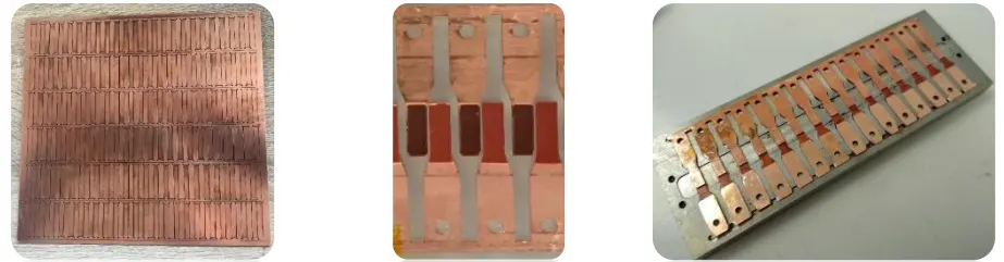
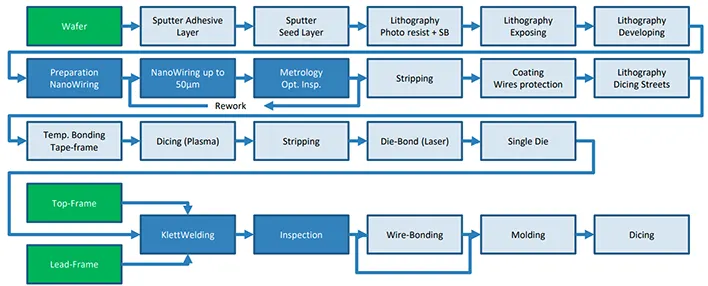
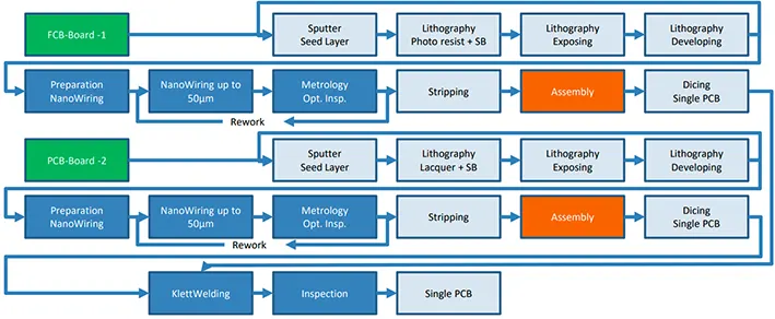
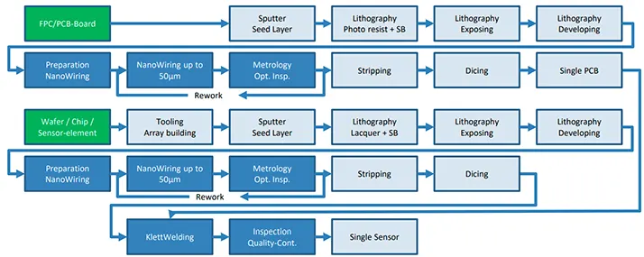
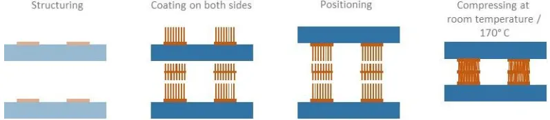
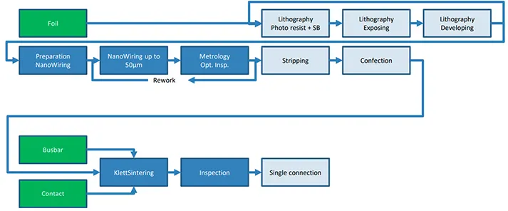
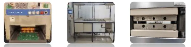
1. Lithography:
- To cover or passivate sensitive surfaces, we use various established processes. Spray coating, laminating lacquer, adhesive tape (Capton), mechanical covers, solder resist. Furthermore, we use laser exposers or mask exposers.
2. NanoWiring
- For NanoWiring, we use our semi-automatic network-based NanoWiring production line. This is a batch machine with a current production area of 300×300 mm². A drawer is inserted into the machine, which then provides appropriate devices for contacting, holding and covering the substrates. NanoWiring is a current-driven process, it is an active galvanic process. The current deflection defines where the NanoWiring should take place.
3. Stripping:
- Currently, we use a bath-based system that runs the substrates through various solvents and cleaning agents to remove everything that is not needed for contact. Adhesion and germ layer are also removed here. We dry the substrates in the decoating unit by air flow.
4. KlettWelding, KlettSintering, KlettGlueing:
- For joining the substrates, standard automatic placement machines are used for small components. Standard pick-and-place machines have a placement force of approx. 8kg with a hook-and-loop welding force of 17MPa, which corresponds to a maximum contact area of 4.7mm². For higher forces, presses such as sintering presses of all kinds can be used. In this case, it must be ensured that the connection is plane-parallel.
5. NanoInspection:
- Either stereomicroscope, SEM, monochromatic microscopy, EDX
| Substrate material | NanoWiring / KlettWelding | KlettSintering |
|---|---|---|
| Ceramics (Al2O3 ) | - Sputtering of metallic seed layers (Ni/Au, Ni/Cu, TiW/Cu, Cr/Cu, etc.) - Vapour deposition of a Ti/Pt/Au layer - Printing and firing silver paste | - Sputtering Metallic layer (Ni/Au, Ni/Cu, TiW/Cu, Cr/Cu, etc.). The metallic - layer must be heat-resistant. Vapour deposition of a Ti/Pt/Au layer - Printing and burning in silver paste The layer must be heat-resistant for Velcro sintering. |
| Silicon | - Sputtering of metallic seed layers (Ni/Au, Ni/Cu, TiW/Cu, Cr/Cu, etc.) - Vapour deposition of a Ti/Pt/Au layer | - Sputtering of metallic seed layers (Ni/Au, Ni/Cu, TiW/Cu, Cr/Cu, etc.) - Vapour deposition of a Ti/Pt/Au layer The layer must be heat-resistant for Velcro sintering. |
| Stainless steel | 1. pre-coating with gold flash 2. optional: pre-coating with copper Electrocoating | 1. pre-coating with gold flash 2. pre-coating with copper electrolyte |
| Aluminium | 1. pre-coating with zincate process 2. pre-coating with copper | 1. pre-coating with zincate process 2. pre-coating with copper |
| Nickel | 1. pre-coating with chemical gold or flash gold 2. optional: Pre-coating with copper | 1. chrome plating with immersion gold from Flash Gold 2. optional: Pre-coating with copper -> If formic acid is used, no pre-treatment is required |
| Chrome | 1. pre-coating with chemical gold or flash gold 2. optional: Pre-coating with copper | 1. pre-coating with chemical gold or flash gold 2. pre-coating with copper |
| Glass (borophosphate) | - Sputtering of metallic seed layers (Ni/Au, Ni/Cu, TiW/Cu, Cr/Cu, etc.) Vapour deposition of a Ti/Pt/Au layer | - Sputtering of metallic seed layers (Ni/Au, Ni/Cu, TiW/Cu, Cr/Cu, etc.) - Vapour deposition of a Ti/Pt/Au layer The layer must be heat-resistant for Velcro sintering |
| Copper, Silver, Gold, Brass | No treatment required | No treatment required |
The process time for NanoWiring depends on the NanoWiring length. In the initial phase, we assume a total process time of 1 hour for a batch run. This time is then reduced to approx. 15-30 minutes in the course of further process optimizations.
For our copper plating process, we use a temperature above room temperature, but below 50°C, so that this ensures at all times that the outside temperature has no influence on the process parameters. Furthermore, the temperature is so low that there is no damage to the substrate materials.
We have integrated an air drying unit into the decoating machine so that after the substrates have been chemically cleaned, the substrate is dried.
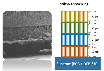
- To increase the thickness of the adhesive joint or to have more flexibility within the joint we can use a NanoWiring stilt. In the stilt NanoWiring process, several layers are stacked on top of each other in multiple NanoWiring runs.
- This results in the thickness of the bond line:
- 𝐛𝐨𝐧𝐝𝐥𝐢𝐧𝐞 𝐭𝐡𝐢𝐜𝐤𝐧𝐞𝐬𝐬 = 𝐧𝐋𝐚𝐲𝐞𝐫 ∗ 𝟓𝟓 µ𝐦
Example
- 2 layers → bondline thickness = 110 µm
- Layers → Bondline thickness = 220 µm
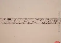
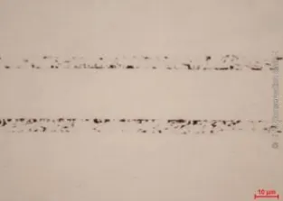
Do you have photos of the cross-section after connection?
We have taken various SEM analyses and micrographs. We can provide you with a selection of images.
Is metal bonding used?
We have joined different metals together. In the NanoWiring structure, we normally always use the same metals in such a way that mixing of metals is not possible. If different metals are to occur directly in the connection zone, we build appropriate diffusion barriers into the structure to prevent mixing.
How can I carry out an electrical test after connecting?
The electrical test can be carried out with a simple resistance meter. The resulting joint is gas and water tight. It has a residual porosity between 1 and 9 %, depending on the joining method. All temperature-influenced joining methods (KlettSintering, KlettSintering+ as well as KlettWelding+) have a tighter joint, KlettWelding, KlettWelding-Underfill, KlettGlueing and KlettGlueing+ have a more porous joint but a higher elasticity.
What equipment do we need to investigate the defects of NanoWiring?
- It is not necessary to invest in high-tech equipment.
- Even a simple stereo microscope worth €150 is enough to detect the errors of
NanoWiring.
4-wire measurement
Is it possible to underfill an assembled 6″- (possibly later 8″-) wafer stack with a bondline thickness of 5-6um?
- We usually apply the low viscosity underfill directly by dispenser to the NanoWiring structure before joining. This is one of the advantages of our technology, that the bond is formed even if the underfill has been applied before.
- Of course, the underfill can also be applied afterwards. But this is certainly more time-consuming. In today's practice, many have to struggle with the fact that the underfill runs only randomly and with little reproducibility between the boundary layers of the substrates. Boundary layer between the substrates.
- Whether 6″" or 8″ is irrelevant for the dispenser application, but it will certainly be a know-how-relevant process.
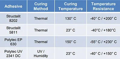
How does the adhesive work in the KlettGlueing process?
- In the KlettGlueing process, the nanowires displace the adhesive and establish the connection to their joining partner.
- The low-viscosity adhesive used (e.g. Structalit 8202) seals the remaining gaps within the joint.
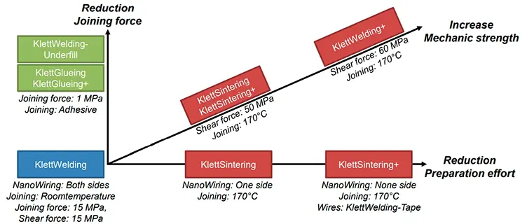
Do you have comparable test data on the influence of strength (tension and shear) under different connection conditions?
- KlettWelding: approx. 15 MPa
- KlettWelding+: approx. 60 MPa
- KlettSintering: approx. 50 MPa
- KlettSintering+: approx. 50 MPa
- KlettGlueing/KlettGlueing+: approx. 10-50 MPa depending on the adhesive used
Shear force: depends on the different end products, what is your experience?
- The resulting shear strength depends mainly on 4 factors: Joining method, joining temperature, joining pressure and joining time. The material also has an influence on the final systemic strength, as the strength of the joint cannot be higher than the basic strength of the material.
- The optimum values for temperature, pressure and time depend on the joining method used and the material of the elements.
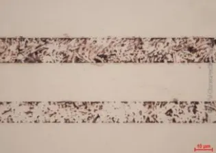
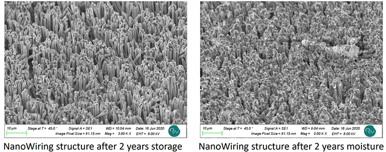
How long can nanowiring structures be stored?
- At present, there are no observations that NanoWiring structures that have been stored for one year
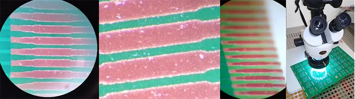
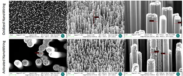
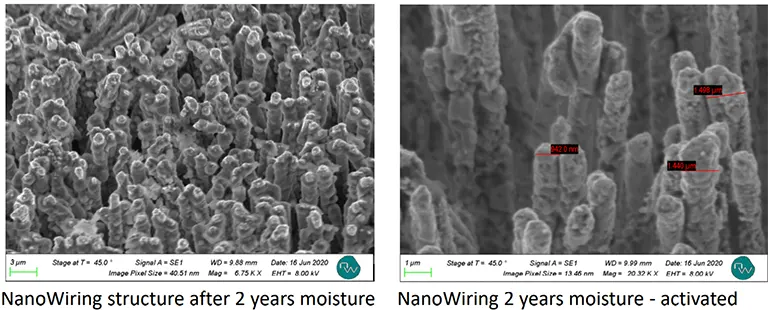
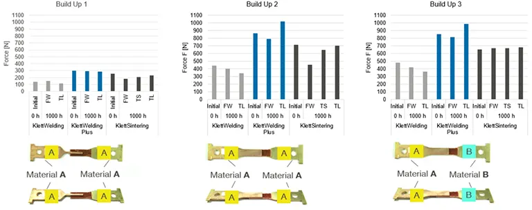
show a change in the connection behaviour, the connection strength or the conductance values. - In the pictures on the left you can see Multi Angle NanoWiring structures that have been stored in a humid environment for 2 years. As can be seen under the SEM, an extremely strong oxidation of the surface has taken place. The surface was cleaned with KlettWelding activator before use. The reduction is clearly visible in the next SEM image, as is the crack in the structure. The KlettWelding tape was then used for a KlettSintering+ process. Subsequent tensile tests / shear tests Shear tests showed no change in tensile strength.
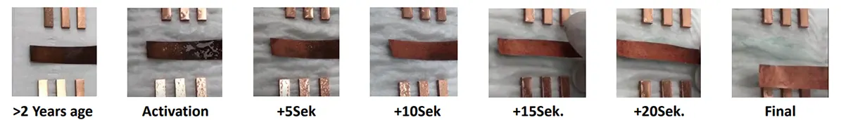
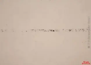
Oxidation after 2 years of normal storage (rectangular tape)
Oxidation after 2 years storage with WATER (Multi-Angle-Tape)
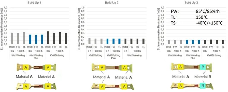
0h / 500h / 1000h
- FW: 85°C/85% rh
- TL: 150°C
- TS: -40°C/+150°C
Is there any impairment of the surface oxide layer?
- We distinguish between two areas in which we serve the topics:
- NanoWiring → As long as we NanoWire copper, residual oxide formation on the surface has a negligible effect. The acidic electrolyte dissolves the oxidation traces so that the process is not affected. In general, a clean and grease-free surface must be available for the NanoWiring process.
- If gold electrolyte is to be used, appropriate care must be taken as the gold electrolyte is not acid-based.
- KlettWelding, KlettSintering, KlettGlueing → Since we do not currently apply oxide-inhibiting coatings to the
NanoWiring structures, we currently always use a KlettWelding Activator to remove the OXID layer on the copper. Light oxidation does not play a role in this process. The layers are mechanically stressed when the hair is woven, so diffusion and contact are still guaranteed. Both commercially available wet chemical and dry chemical processes are available for the reduction; alternatively, hydrogen plasma can also be used.
Do we need plasma treatment as a surface treatment before NanoWired processing?
- Generally not. If we have done an organic treatment, for example through lithographic processes, we use oxygen plasma to remove all organic residues.
- Before hook-and-loop welding, we currently activate the surface with hook-and-loop welding activator or hydrogen plasma.
Do we need reduction treatment, flux, etc. when we make a connection?
At the moment we are doing this, but we are evolving so it will not be necessary in the future.
Is there an alloy formation or not?
We try to design the joint in such a way that only purely metallic structures are used in the KlettWelding /
KlettSintering / KIettGlueing Zone only pure metal structures are to be found, or corresponding nickel diffusion barriers are planned in.
Do you have the results of the reliability test after connection (to confirm the resistance value change of TC, etc.)?
- We carried out reliability tests especially for KlettWelding+, KlettSintering and KlettSintering+. For this purpose, the samples were stored at 150° C and the electrical and mechanical strength was tested after "0h", "500h", "1000h" and "4000h". "In parallel, the same analyses were carried out at 85° C and 85% relative humidity and at a temperature change between -50° C and 140° C.
- All these tests show that the quality of the connections is not affected under load.
- In addition, NanoWired is currently conducting a study where our customers can purchase 10T€, which will run for one year and intensively analyze the behavior during ageing and storage.