KlettWelding
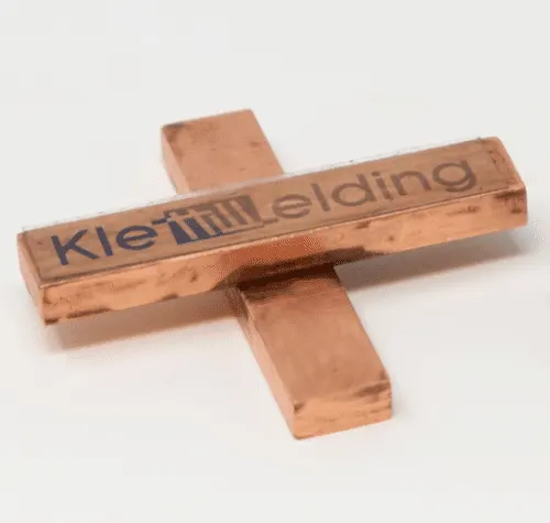
The metallic Velcro fastener
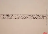
Both surfaces have a NanoWiring structure
Shear strength up to 60 MPa
Resulting bond has electrical and thermal characteristics comparable to bulk metal
KLETTWELDING PROCESS
How We Manufacture KlettWelding
Structuring
Coating
Both surfaces have a NanoWiring structure
Positioning
Compressing
Room temperature
Pressure from 15 MPa
Time from 60 ms

KLETTWELDING OVERVIEW
KlettWelding Applications
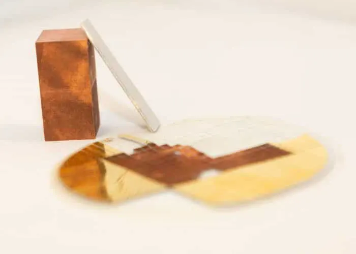
Flip chip
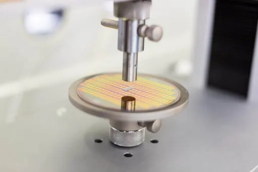
Semiconductor production
Assembly joints - FPC/PCB, PCB/PCB
Plastic connections
Die Attach
Temperature sensitive devices
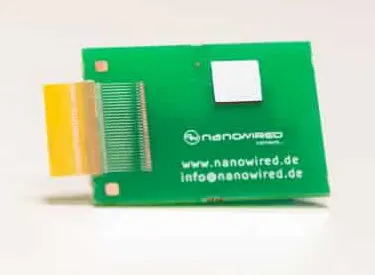
KlettWelding Video Tutorial
Watch video about KlettWelding presented by our CEO
KLETTWELDING+ PROCESS
KlettWelding+
Highest connection strength
Both surfaces have a NanoWiring structure
KlettWelding Applications
Die attach
Flip chip
High current busbars
How We Manufacture KlettWelding+
Structuring
Coating
Both surfaces have a NanoWiring structure
Positioning
Compressing
From 170°C
Pressure from 10 MPa
Time from 10 s

Comparison of NanoWired connection technologies
The following tables shows the comparison between KlettWelding and KlettWelding+ connection technologies
KlettWelding
KlettWelding+
NanoWiring
Both Sides
Both Sides
Process Temperature (°C)
20
170...240
Process Pressure (MPa)
From 15
From 10
Process Time (s)
0.06...60
120...300
Shear Strength (MPa)
6...20
20...65
Main Advantage
Very fast
Very fine pitch
Low temperature
Very fine pitch
Low temperature
Very fine pitch
Very high shear strength
Very high shear strength
Typical Application
Die Attach
Flip Chip
Temperature sensitive devices
Flip Chip
Temperature sensitive devices
Die Attach
Flip Chip
High current busbar
Flip Chip
High current busbar