2D/3D Packaging
Stress-free joining of thin film wafersBonding of Hybrid systems High mechanical unevenness is tolerated
ADVANCED TECHNOLOGY
Process Advantages
<0 sec
High Speed Cu-Sintering
0°C
Low Temperature Process
<0um
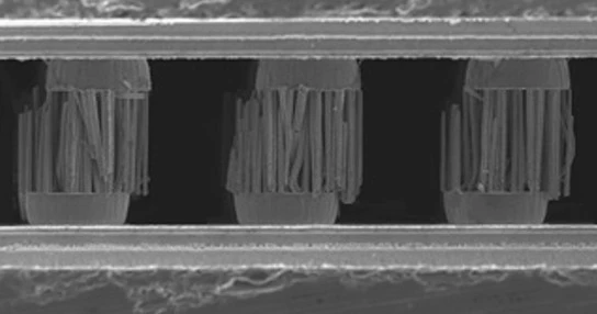
Bond Line Thickness
Fast Process
● Process could be done under 1 minute
Easy Process
● No Printing/Dispensing
● No Drying
● No Cleaning
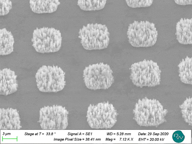
Filling Up Irregularities
High mechanical unevenness is tolerated (>>10µm)
Excellent Bond Properties
● Bond line thickness <<3µm => Lowest inductivity
● Stress-free joining of thin film wafers
● 3µm – 300mm Contact 0Ω
● One Step- D2D, D2W, W2W Process
● Room temperature process KlettWelding