KlettSintering
Robust substrates, strong connection
Most cost-effective method
Only one surfaces have a NanoWiring structure
Shear strength up to 60 MPa
Significantly higher tensile strength than KlettWelding


KLETTSINTERING PROCESS
How We Manufacture KlettSintering
Structuring
Coating
One surface has a NanoWiring structure
Positioning
Compressing
From 170°C
Pressure from 10 MPa
Time from 10 s

KLETTSINTERING OVERVIEW
KlettSintering Applications
Automotive busbar Power transport by car/plane/truck
Housing technology
Power Electronics / Die Attach
Contact link
Ceramics on metal (e.g. sensors)


KlettSintering Video Tutorial
Watch video about KlettSintering presented by our CEO
KLETTSINTERING+ PROCESS
KlettSintering+
Minimum preparation effort
No surface has NanoWiring structure
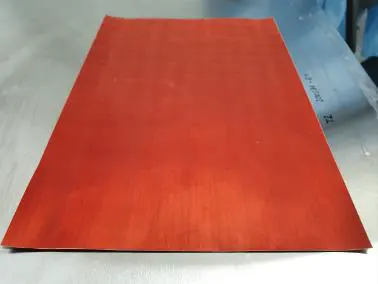
Use of KlettWelding Tape
High-strength, repairable
KlettSintering+ Applications
Highest flexibility application
High current busbars
3D electronics
How We Manufacture KlettSintering+
Structuring
Coating
No surface has NanoWiring structure
Positioning
Compressing
From 170°C
Pressure from 10 MPa
Time from 120 s

Comparison of NanoWired connection technologies
The following tables shows the comparison between KlettSintering and KlettSintering+ connection technologies.
KlettSintering
KlettSintering+
NanoWiring
One Side
KlettWelding Tape
Process Temperature (°C)
170...240
170...240
Process Pressure (MPa)
10...30
10...30
Process Time (s)
120...300
120...300
Shear Strength (MPa)
20...50
30...60
Main Advantage
High shear strength
Very fine pitch
Only one NW level
Very fine pitch
Only one NW level
No NW stage
High shear strength
High shear strength
Typical Application
Die Attach
Flip Chip
Flip Chip
Die Attach
Flip Chip
High current busbar
Flip Chip
High current busbar